- Part I: CPU (6507)
- Part II: Cartridge
- Part III: TIA (Video chip)
- Part IV: Clock and Composite Video
- Part V: RIOT (RAM, I/O, Timer) and Audio
- Part VI: Joystick, switches, fixes and wrapping up
Tidying Up
In the previous posts I made the CPU work on the breadboard, then added a cartridge connector, all using jump wires - which can be easily reconnected, labeled, etc., but have a downside: they disconnect easily. Coupled with the equally flimsy cart connector, all my attempts at moving on with the project would result in failures.
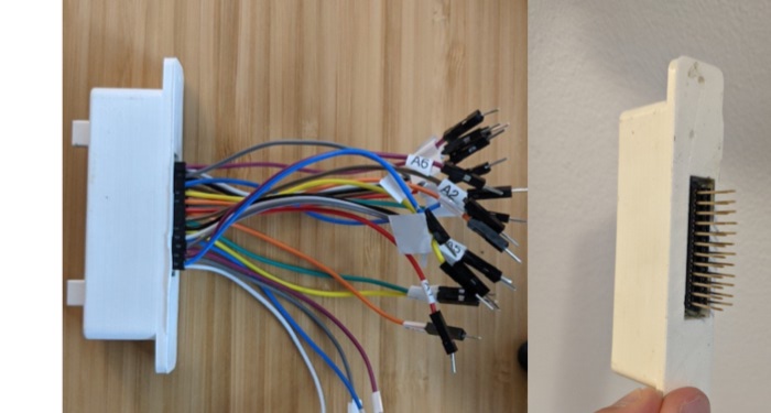
After seeing Ben Eater’s beautiful breadboard computers I decided to rewire the boards I already had. For that, I’d have to rethink my cartridge connector: instead of having the jumper cables going out of it (left), I got some long pin female headers that extended the pins so the connector now fits the board like any other chip (right):
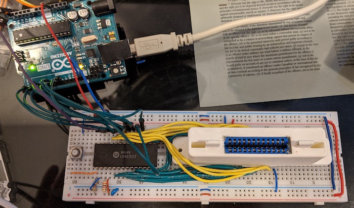
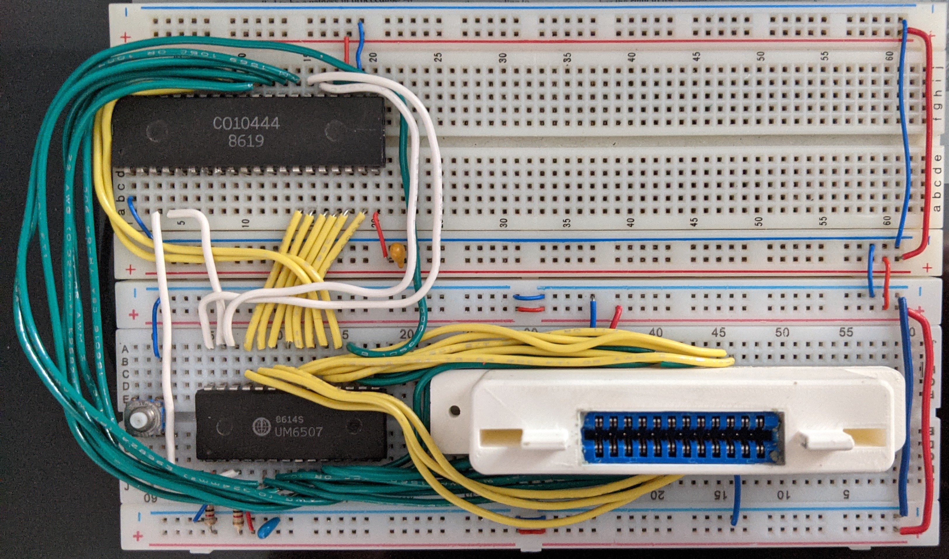
Armed with that and Ben’s video with tips, I rewired everything I had (minus the “pause” button, as it will be replaced on the next step). Other than the Arduino (which is temporary), everything is now nice, tidy and color-coded (data is yellow, addresses are green, +5V is red and ground is blue):
Wiring the TIA
The Television Interface Adapter (TIA) is the only custom chip on the Atari. It was designed to generate the video and audio signals, and to reduce costs, it has nearly no video memory, requiring programmers to sync their code with the TV signal - with microssecond precision. To aid in that task, the TIA controls the 6507 CPU in two ways:
- It provides the CPU clock, by “dividing” its input clock by 3, that is: for every three pulses that the TIA receives from the clock crystal (for now, in our case, from the Arduino), it sends one pulse to the CPU.
- When the software writes to the
WSYNCaddress, the TIA halts the CPU (using theRDYpin) until the current scanline in the video finishes drawing.
For that magic to work, we need to connect the 6507 clock pins (ø0 and ø2; the later is an output that seems to help keeping things in sync) and the RDY pin to their matching TIA pins (keeping the pull-up resitor); we’ll also connect the R/W pin between them (so the TIA can know whether the 6507 wants to read or write to it).
And, of course, connect the data pins (D0-D7) and the lower address pins (A0-A5), so the data can flow from/to the proper addresses. Finally, connect two address pins and two fixed voltages to the “chip selector” TIA pins (CS0-CS3), so TIA knows when the CPU is talking to it (as opposed to the cart or the other upcoming chip).
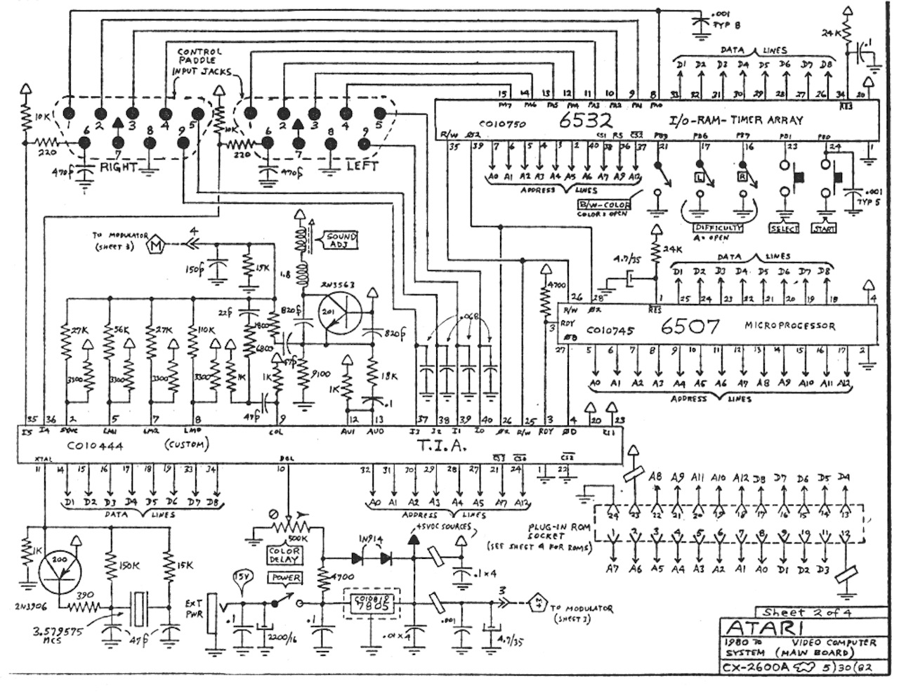
I found some TIA pin descriptions online, but they had a few incorrections; so I guided myself mostly on the original schematics and built this table for TIA-to-CPU connections:
| Pin Name | TIA # | 6507 # |
|---|---|---|
ø0 |
4 |
27 |
ø2 |
26 |
28 |
RDY |
3 |
3 |
R/W |
25 |
36 |
D0 |
14 |
25 |
D1 |
15 |
24 |
D2 |
16 |
23 |
D3 |
17 |
22 |
D4 |
18 |
21 |
D5 |
19 |
20 |
D6 |
33 |
19 |
D7 |
34 |
18 |
A0 |
32 |
5 |
A1 |
31 |
6 |
A2 |
30 |
7 |
A3 |
29 |
8 |
A4 |
28 |
9 |
CS0/A12 |
24 |
17 |
CS3/A7 |
21 |
12 |
and one for the direct-to-power connections:
| Pin Name | TIA # | +/- |
|---|---|---|
CS1 |
23 |
+5V |
CS2 |
22 |
GND |
VSS |
1 |
+5V |
VCC |
20 |
GND |
Throwing a 100nF capacitor close to the VSS pin gives the TIA clean power (like I did to the CPU). I stacked a second breadboard on the first to add the TIA, using the same color conventions of before for power, data and address signals, adding white for non-address/non-data TIA-to-CPU connections.
I aligned the TIA with the breadboard numbers, which proved to be a mistake: several cables needed to go through the left side and had to hang outside of the board. Other than that, it looks pretty nice:
Testing
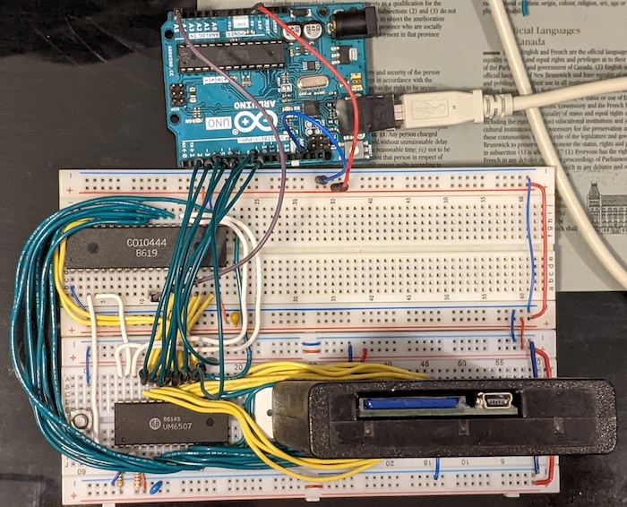
Once again, I’ll plug an Arduino for testing, connecting pins 2-9 to the data lines as in the previous post. This time, I’ll connect the Arduino-generated clock pin to the TIA clock input (OSC, pin 11), and slightly reduce the delays to 10ms, speeding the clock to roughly 50Hz (still around 24 times slower than the real Atari):
// Turns an Arduino into a 50Hz clock generator (on pin A5)
// and a monitor for an 8-bit data bus (pins 2-9)

void setup() {
  for(int pin = 2; pin <= 9; pin++) {
    pinMode(pin, INPUT);
  }
  pinMode(A5, OUTPUT);
  Serial.begin(115200);
}

void loop() {
  // Clock pulse
  digitalWrite(A5, HIGH);
  delay(10);
  digitalWrite(A5, LOW);
  delay(10);

  // Print current data bus (pins 2-9)
  int data_value = 0;
  int power_of_two = 1;
  for(int bit = 0; bit <= 7; bit++) {
    data_value += digitalRead(bit + 2) * power_of_two;
    power_of_two *= 2;
  }
  if (data_value < 0x10) { Serial.print("0"); }
  Serial.println(data_value, HEX);
}
Instead of an actual game, this time I loaded my Harmony Cart with the Atari 2600 Hello, World program that I created once for an Atari 2600 Programming presentation, because we don’t have RAM or timers yet, and that software doesn’t use either.
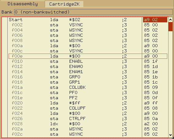
Once again, let’s have the Stella disassembly handy:
and check the Arduino output (right after we reset the CPU with the button on the breadboard). This time I’ll remove the timestamps, group the numbers together and put on a Gist, to make it easier to analyze:
First thing to notice: that almost all numbers print three times. That is expected: the TIA sends one clock pulse for each three it receives, and we monitor the data lines every time we send a clock pulse to TIA.
When we account for the triple vision, the output is not unlike the one on the previous post: line 1 shows the 6502 reading the two-byte location of the reset vector on the cart (F000, read in reverse order). Line 2 matches the instruction at that address (LDA #$02, that is, A9 02 in machine code), and line 3 is the following instruction (STA VSYNC, or 85 00). The STA writes the value 02 to memory, which takes an extra cycle (line 4, with the 02 forming at the end of the cycle).
Things get odd at lines 7, 10 an 13, where we see a lot of repeated numbers. What gives? Well, the lines above them are STA WSYNC, and as stated above, when we write to that address, TIA uses the RDY pin to “freeze” the 6502 until an entire scanline is produced; which is why the data bus didn’t change until we total 228 cycles.
If you pay attention, you may notice that we have a little less than that number of bytes on lines 10 and 13, and even less on line 7; that is because we have to discount the cycles “spent” since the current scanline started.
Anyway, this more than proves that our TIA is up and running!
Next
One may wonder why I don’t plug this on the TV, given there is a video chip. We’re missing a couple things that I plan to add on the next post, in which I expect to finally generate some image!