- Part I: CPU (6507)
- Part II: Cartridge
- Part III: TIA (Video chip)
- Part IV: Clock and Composite Video
- Part V: RIOT (RAM, I/O, Timer) and Audio
- Part VI: Joystick, switches, fixes and wrapping up
Introduction
A year ago, Ben Heck hand-soldered an Atari 2600 on a protoboard (and, as usual, turned that into a portable console). The idea of manually re-assembling the console for which I had already hacked together a game and an emulator sounded very exciting (and educational) for me.
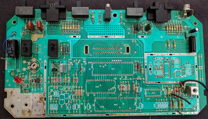
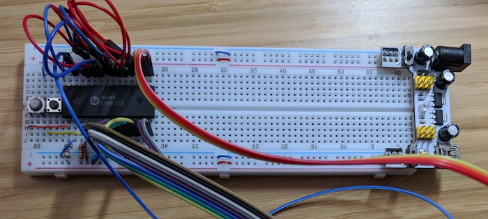
The show crew always publishes schematics for his projects, so while I waited for that, I started de-soldering the chips and cartrige conector (and a few extra components, why not?) from an old Atari Jr. board I had lying around. De-soldering is hard, but eventually it was done:
The schematics, however, never came. That episode’s GitHub repository only includes the original Atari’s block diagram, so I shelved the plan. But more recently I stumbled upon a series of blog posts in which David Barton describes how he built a 6502-based computer (a 65c02, to be precise) on a solder-less breadboard.
Those boards aren’t as sturdy or portable as traditional printed circuit boards, but the freedom to tinker (and make mistakes) sparked my flame once again, so I decided to give the project another shot. I started by reproducing his first two posts, but adapted to the Atari’s 6507 and adding a couple tweaks.
Building
The first step was to position the 6507 on the breadboard - easy, yet I managed to mess up. I aligned the 6507 first pins with the numbered tracks, which sounds smart, but leaves little space to work on the first/last pins. If you are trying this, put the chip closer to the center and save yourself the trouble.
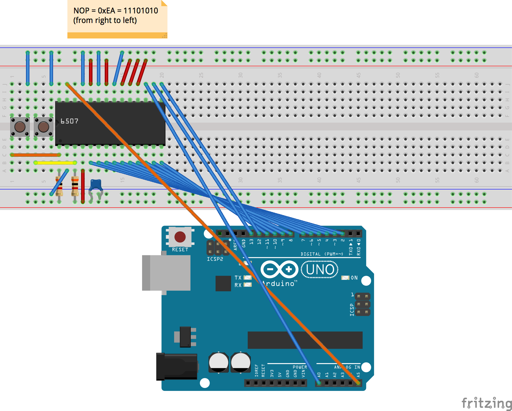
The connections are roughly the same as Barton’s project, but translated to the 6507 pin layout. 5V power goes to pin 4 (VCC) of the 6507, and ground goes to pin 2 (GND). There is no IRQ or NMI, so you only need two 3K resistors coming from 5V - one ending on the reset input (pin 1) and another on RDY (pin 3).
Also following him, I added a push button between the ground and the reset pin, so I could (re-)start the processor at will. The 6507 seems to work without that, but it didn’t hurt. But I also added a second push button between ground and RDY - this one is more interesting, you’ll see later why.
Still on his footsteps, I added the decoupling capacitor (a 100nF, 20V non-polarized ceramic) close to the power pin, to ensure clean power to the chip. Finally, I hard-wired the binary value 11101010 to the data pins, by connecting 18, 19, 20, 22 and 24 (the 1s) to 5V and pins 21, 23 and 25 (the 0s) to ground. It sounds like an arbitrary value, but it will also make sense later. For now, just keep in mind that this makes CPU “believe” it is connected to a ROM chip where every single byte is 11101010 (or 0xEA in hexadecimal).
Here is the first version of the finished job. It isn’t super easy to follow (even in higher resolution, but check the UPDATE session below for a cleaner version and a drawing):
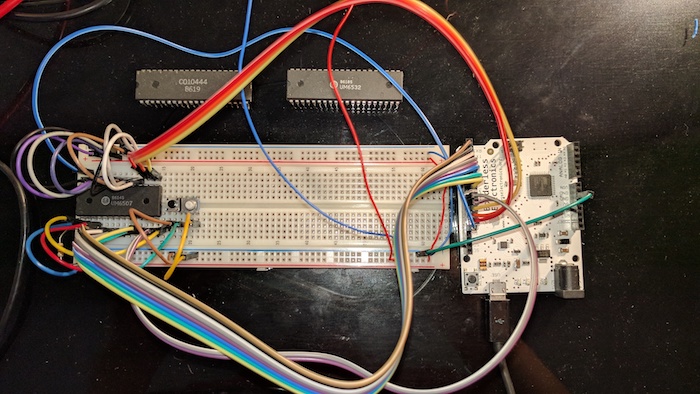
You may notice the other two Atari chips above (should have labeled them “SOON” 😎) and, more important, an Arduino wired to the breadboard. It has two functions:
- Generate a clock pulse (an impractically sluggish one for real usage, but great for our experience);
- Monitor the address lines, feeding the results to a trusty PC (or Mac), so we can check which memory address the CPU is trying to read.
I changed his code to read all 13 address bits on the 6507 (using Arduino’s digital pins 0-12, wired to the same-numbered 6507 address lines) and send the clock pulse via Arduino digital pin 13 (so I could “see” the clock pulses on my board’s built-in LED, which is hard-wired to that pin).
Playing
When I turned it on, I only got garbage.
To be precise: it worked as I expected for a few cycles, then went crazy. After pulling lots of hair that I don’t have, I figured the culprit: clock speed.
Barton’s code makes one clock pulse every second (i.e., 1Hz), which may be fine for a “modern” 65c02, but my old-school 6507 could not hold its state running that slow. Changing delay(1000) to delay(100) on his code gave our chip a blazing 10Hz speed - fast enough for it not to get lost, yet slow enough for human eyes to watch (without an oscilloscope).
(also less than 1/100,000th of an actual Atari’s speed, FWIW)
Here is the modified code (gist):
Now comes the really fun part: watching the CPU work. With the power off, all pins on the address bus read as 0 bits, so the Arduino output starts like this:
Lower address bus : 0000000000000 : 0x0
Lower address bus : 0000000000000 : 0x0
Lower address bus : 0000000000000 : 0x0
Lower address bus : 0000000000000 : 0x0
When we turn the breadboard power on, things change a bit. First the CPU reads (or writes, who knows) a few addresses (most on the 0x01xx range, hinting a stack-related operation akin to the 6502 reset).
Lower address bus : 0101000000000 : 0xA00
Lower address bus : 0101000000000 : 0xA00
Lower address bus : 0000100000000 : 0x100
Lower address bus : 0000111111111 : 0x1FF
Lower address bus : 0000111111110 : 0x1FE
What really matters comes now: it reads the contents of the the addresses that match the NMI vector (canonically 0xFFFA and 0xFFFB, but we only have 13 address pins, so that will become 0x1FFA and 0x1FFB):
Lower address bus : 1111111111010 : 0x1FFA
Lower address bus : 1111111111011 : 0x1FFB
Honestly, I’d expect it to read the RESET vector (0xFFFC and 0xFFFD). But that must be why Atari carts have all all vectors pointing to the beginning of the code, not just RESET. Anyway, when you turn on the console, the CPU reads the address stored in those two bytes of the cartridge and starts running code from that address.
In our breadboard, the CPU will always read the value 0xEA (because we wired its data bus to its binary value of 11101010, remember?). So it assumes our “game” actually starts at the address 0xEAEA (1110101011101010), and starts reading code from there.
Once again, keep in mind we only have 13 bits on the address lines, so the actual address becomes 0000101011101010, or 0x0AEA:
Lower address bus : 0101011101010 : 0xAEA
Lower address bus : 0101011101011 : 0xAEB
What happened now? Well, the CPU requested the contents of 0xAEA, but our breadboard’s response to any memory read is always the same: 11101010, or 0xEA. It just so happens that this value is the opcode of the NOP instruction, which tells CPU to do nothing (NOP = No OPeration), and just move on to the next memory address.
So the CPU did that, reading 0xAEB. But 0xAEB will also contain an NOP (every address will).
Can you guess the result?
Lower address bus : 0101011101011 : 0xAEB
Lower address bus : 0101011101100 : 0xAEC
Lower address bus : 0101011101100 : 0xAEC
Lower address bus : 0101011101101 : 0xAED
Lower address bus : 0101011101101 : 0xAED
Lower address bus : 0101011101110 : 0xAEE
Lower address bus : 0101011101110 : 0xAEE
Lower address bus : 0101011101111 : 0xAEF
Lower address bus : 0101011101111 : 0xAEF
...
We see each line twice because our monitor dumps the current addres at every CPU clock cycle, and the NOP instruction takes two cycles to run. This “free run” is said to be a rite of passage for computer builders. We had a good start, and could just pop the champagne.
But wait, there is more! Remember we added a button to pull down the RDY pin? If we press it, the CPU will ignore the clock cycles, but keep its state - in other words, it will pause.
Check it out - the CPU is there, free-running:
...
Lower address bus : 0101100010001 : 0xB11
Lower address bus : 0101100010010 : 0xB12
Lower address bus : 0101100010010 : 0xB12
Lower address bus : 0101100010011 : 0xB13
Lower address bus : 0101100010011 : 0xB13
Lower address bus : 0101100010100 : 0xB14
Lower address bus : 0101100010100 : 0xB14
Around here I pressed the button…
Lower address bus : 0101100010101 : 0xB15
Lower address bus : 0101100010101 : 0xB15
Lower address bus : 0101100010101 : 0xB15
Lower address bus : 0101100010101 : 0xB15
Lower address bus : 0101100010101 : 0xB15
…and the value doesn’t change anymore, until the button is released - when it continues as nothing happened:
Lower address bus : 0101100010101 : 0xB15
Lower address bus : 0101100010110 : 0xB16
Lower address bus : 0101100010110 : 0xB16
Lower address bus : 0101100010111 : 0xB17
Lower address bus : 0101100010111 : 0xB17
Lower address bus : 0101100011000 : 0xB18
Lower address bus : 0101100011000 : 0xB18
...
For Atari programmers, this will sound familiar: Atari games need to sync their code with the scanlines that are drawn on the TV at a fixed speed, so they often write to the WSYNC address of TIA (the video chip) to halt the 6507 until the next scanline starts drawing. The TIA simply does what our finger did: sets that 6507 pin to GND until it has finished the current line.
Next steps
My long-term goal/wish is to build an entire Atari on the breadboard. But I’m learning as I go, so who knows where I’ll get?
Anyway, I think the next steps should be:
- Wiring the cart connector (so I could get some actual code running);
- Including the 6532 (also known as RIOT, for providing RAM, I/O and Timers);
- Adding a joystick (or some push buttons to that effect) and console switches;
- Putting a real clock (or a more powerful software one - it would be cool to change the velocity on-the-fly)
- Adding the TIA (likely the most complex part, given it will have to output the video signal somehow)
Feasible? We’ll see, we’ll see.
UPDATE
Building from description may be a bit confusing, so I made a Fritzing (.fzz) drawing:
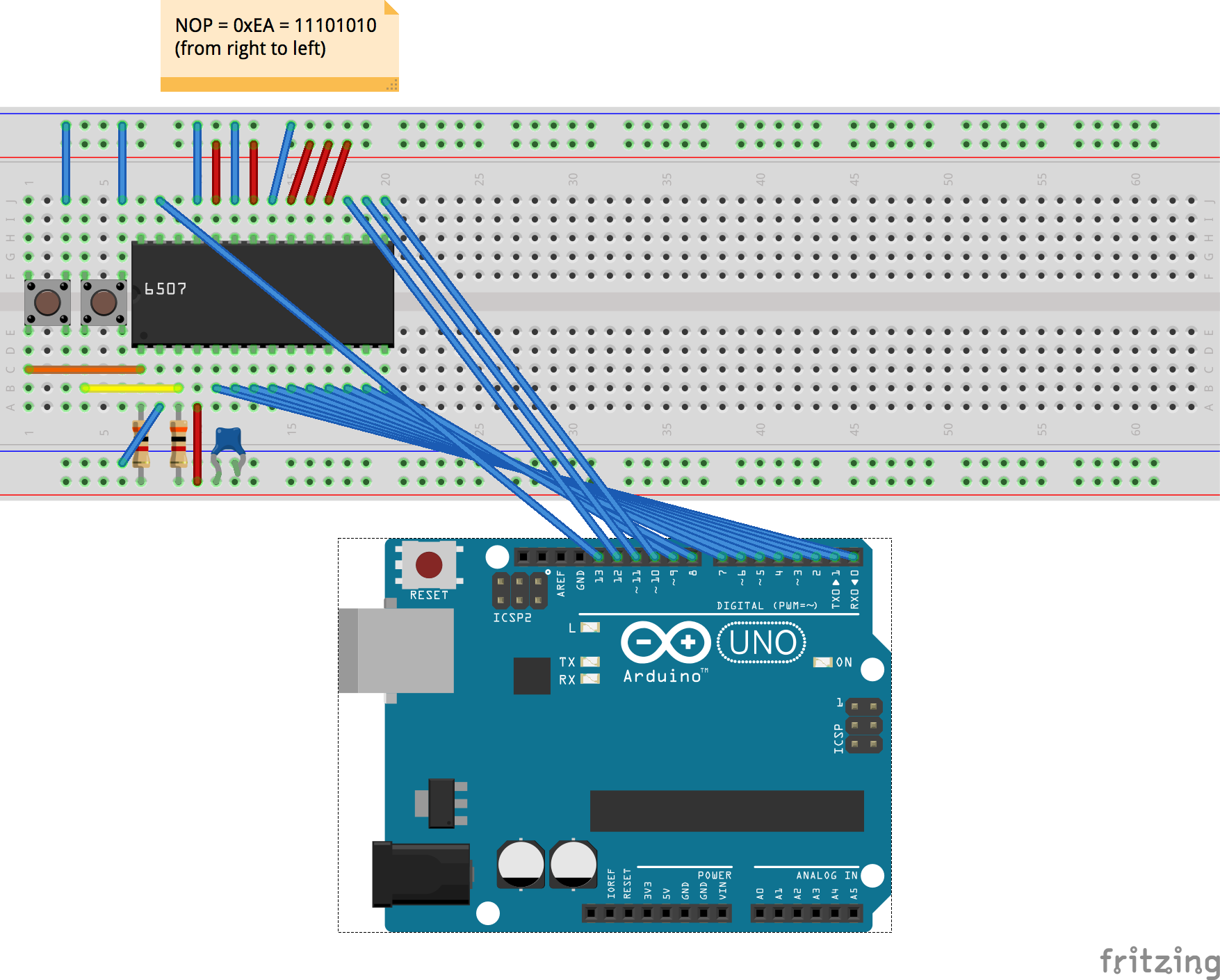
From that drawing, I rebuilt the experiment to weed out the last errors (🙏 ). Using shorter pieces of wire (except for the NOP and the Arduino connection, which will be removed as I add the other chips) and proper colors (red/blue for the 5V/GND connections, for example) resulted in a cleaner build:
ERRATA
A few years later, I’ve rebuilt this in order to figure out the next steps. And, of course, there was one last error!
I was having a hard time uploading the monitor for the second time, and noticed the last couple bits were a bit unstable. It turns out you should not use Arduino pins 0 and 1 if you are dumping serial output.
I am not sure how I managed to make this work before (maybe I was using a compatible board that did not reserve those pins for serial I/O), but I’ve changed the circuit to instead use pins 2-14, where “14” is actually analog pin A0 (which can be used as digital), and pin A5 for the clock.
I’ve also rewrote the monitor program, cleaning it up a quite a bit and printing actual ROM addresses:
// Turns an Arduino into a 10Hz clock generator (on pin A5)
// and a monitor for a 13-bit address bus (on pins 2-14, where 14=A0)

void setup() {
  pinMode(A5, OUTPUT);
  Serial.begin(115200);
}

void loop() {
  // Clock pulse
  digitalWrite(A5, LOW);
  delay(50);
  digitalWrite(A5, HIGH);
  delay(50);

  // Print current address assuming Atari ROM (higher bits all 1s)
  word address_value = 0b1110000000000000;
  for(int bit = 0; bit <= 12; bit++) {
    address_value += digitalRead(bit + 2) * pow(2, bit);
    // EDIT: that code was printing an odd result - you may have better luck
    //       replacing the line above with the one below (thanks, Palako!)
    // address_value |= (digitalRead(bit+2) << bit);
  }
  Serial.print(address_value, BIN);
  Serial.print(" = 0x");
  Serial.println(address_value, HEX);
}
On the board, just skip Arduino pins 0 and 1, wiring pin 2 to CPU A0, pin 3 to CPU A1, …, pin 13 to CPU A11, then pin A0 to CPU A12. Then wire pin A5 to CPU clock. Or just follow the fixed Fritzing (.fzz) drawing:
It seems to work all right now. I still get a couple odd results (notably, 0xFFFB and 0xFFFC instead of 0xFFFC and 0xFFFD read when I press the RESET button, and the last ROM address being skipped), but they may be either 650x oddities, or imperfections from this monitor (EDIT: it may have been indeed an error on the monitor code, see Palako’s comment below). Still, that puts me back on track to continue building up towards the Atari.
Comments
Palako
Hey,
I'm following your series of articles and finding it very useful.
I assume after all this time you won't need this, but for the benefit of future readers, the problem you are having with seeing 0xFFFB and 0xFFFC instead of 0xFFFC and 0xFFFD is a line of code in your Arduino monitor:
address_value += digitalRead(bit + 2) * pow(2, bit);
Change that for:
address_value |= (digitalRead(bit+2) << bit);And everything will make sense.
Thanks again for the articles!
chesterbr
Hello! You are absolutely right, good chances there is a snafu there. I'll keep the original as-is (the following parts focus on the data bus anyway, where the binary conversion seems to be working), but added a note to the text, pointing readers down here. Thank you very much!